Research Vision
Our research explores how emerging materials and advanced device engineering can shape next-generation electronic technologies. By combining low-dimensional materials, semiconductor device design, and fundamental physics, we investigate how charge, spin, lattice, and interface effects interact at the nanoscale. These interactions often give rise to physical phenomena that cannot be observed in conventional bulk materials.
By understanding these mechanisms, we aim to design and engineer nanoscale electronic and spintronic devices with improved efficiency, novel functionalities, and enhanced performance for future computing technologies.
1. Two-Dimensional (2D) Materials
Two-dimensional (2D) materials are crystalline solids that are only a few atoms thick. Unlike conventional materials, their surfaces form atomically sharp interfaces without dangling bonds, making them ideal building blocks for clean heterostructures and novel device architectures. This property allows researchers to combine very different materials in ways that are difficult to achieve in conventional bulk systems.
The field of 2D materials began with the discovery of graphene, a single layer of carbon atoms arranged in a honeycomb lattice. Graphene exhibits extraordinary properties, including extremely high electrical conductivity, exceptional mechanical strength, and unique quantum transport behavior. Its discovery opened a new frontier in condensed matter physics, nanotechnology, and advanced electronics.
Following graphene, a large family of transition metal dichalcogenides (TMDCs) has attracted significant attention, including materials such as MoS₂ and WS₂. Unlike graphene, many TMDCs are semiconductors with sizable bandgaps, making them promising candidates for transistors, photodetectors, and other electronic or optoelectronic devices. Their strong spin–orbit coupling and valley-related properties also provide exciting opportunities for exploring new quantum phenomena.
More recently, the 2D material family has expanded to include nitrides and other emerging compounds, such as hexagonal boron nitride (h-BN), AlN, MoN, and W₅N₆. These materials offer a wide range of functionalities, from atomically flat insulating layers and protective barriers to platforms with potentially novel electronic, magnetic, or superconducting properties.
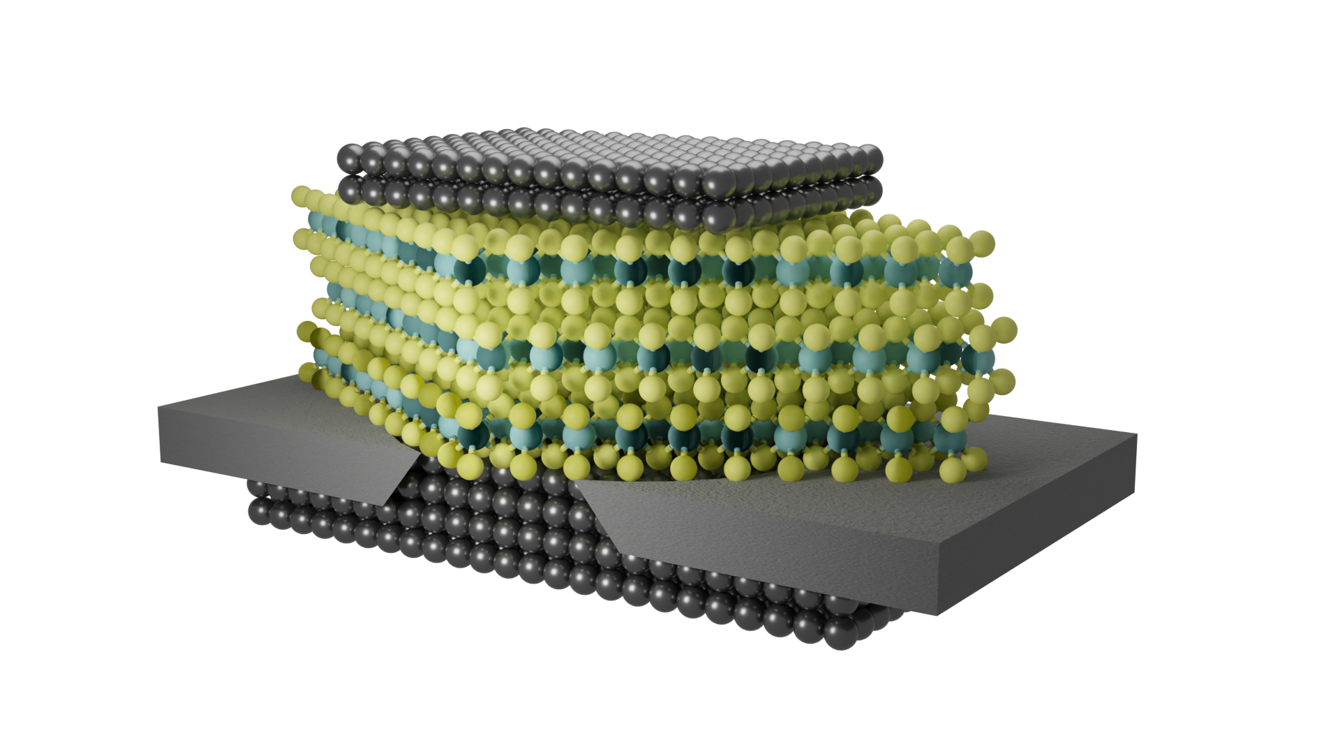
One of the most powerful features of 2D materials is that they can be assembled like Lego bricks. By stacking different atomic layers together, researchers can create van der Waals heterostructures in which each layer contributes a distinct function. These structures provide a versatile platform for studying interactions among charge, spin, lattice, and light, while also enabling new possibilities for electronic, spintronic, and quantum devices.
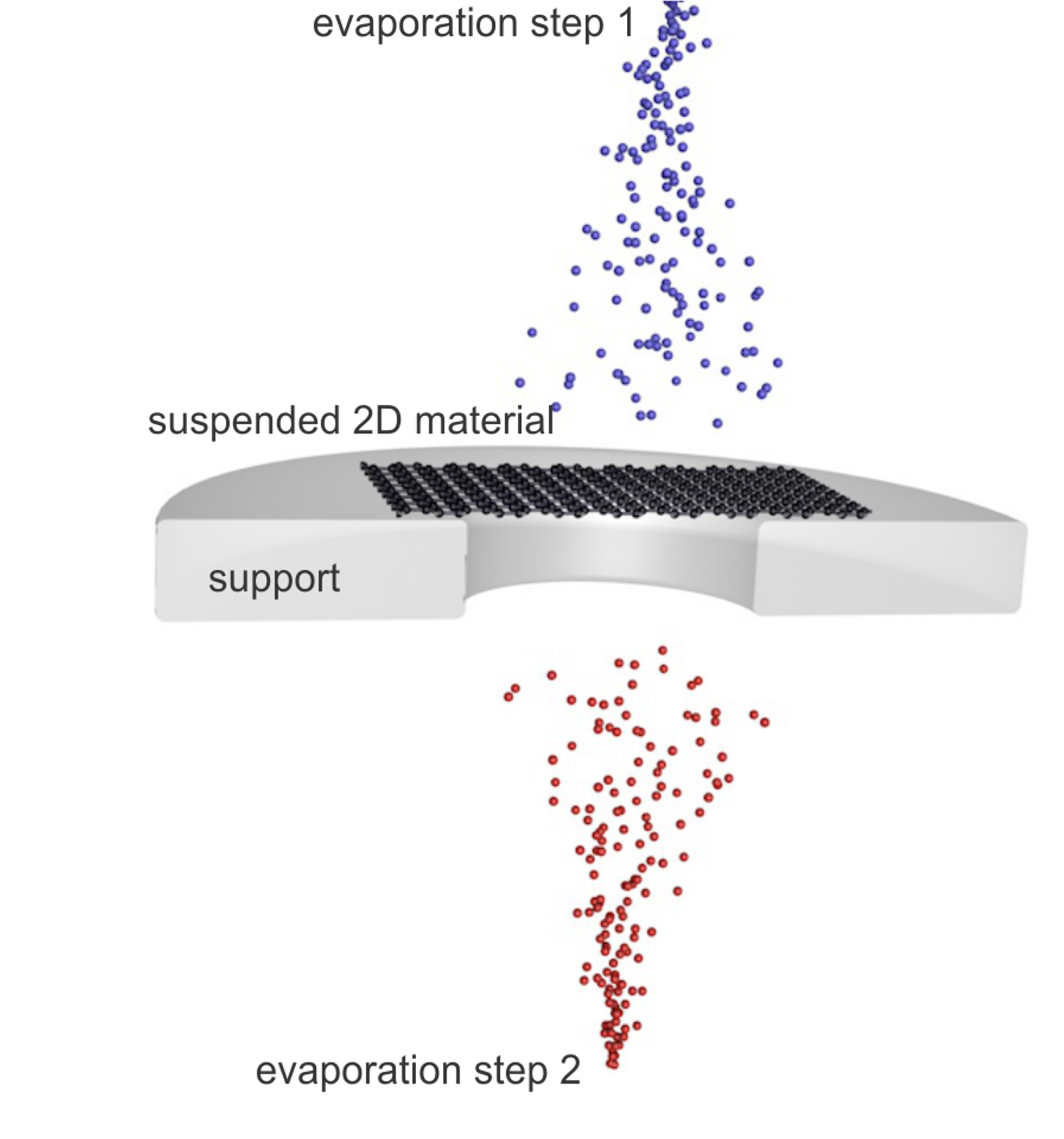
We develop advanced fabrication processes that create ultra-clean interfaces in two-dimensional material devices, enabling higher-quality heterostructures and improved device performance.
2. Electronic and Spintronic Devices
Modern electronic devices operate by controlling the flow of charge in semiconductor materials. Transistors, diodes, and integrated circuits form the foundation of today’s information technologies, enabling computing, communication, and sensing systems that shape modern society. As device dimensions continue to shrink and performance demands increase, understanding charge transport at the nanoscale becomes increasingly important.
Beyond conventional electronics, spintronics introduces an additional degree of freedom: the electron spin. While traditional devices rely solely on charge transport, spintronic devices utilize both charge and spin to store, process, and transmit information. This approach enables new functionalities such as non-volatile memory, magnetic sensing, and energy-efficient logic devices. Technologies such as magnetic tunnel junctions (MTJs) and spin valves have already demonstrated practical applications in modern memory and data storage systems.
Two-dimensional materials provide exciting opportunities for advancing both electronic and spintronic devices. Their atomically thin nature allows precise control of interfaces and electronic structures, which is crucial for efficient charge transport and spin manipulation. When integrated with magnetic materials or engineered heterostructures, these systems can reveal new transport phenomena and enable novel device concepts.
By integrating novel materials, interface engineering, and device physics, we aim to design next-generation electronic and spintronic devices that are faster, more energy-efficient, and capable of entirely new functionalities.
Two-dimensional materials provide new transport modes for electronic and spintronic devices, enhancing operational efficiency, functionality, and emerging opportunities for future technologies.
3. Fundamental Physical Mechanisms
To understand how electronic and spintronic devices operate at the microscopic level, our research focuses on uncovering the fundamental physical mechanisms governing charge and spin transport. We approach this challenge from three complementary perspectives: light, electricity, and magnetism.
Optical techniques such as Raman spectroscopy allow us to probe lattice vibrations and interactions among electrons, phonons, and spins in low-dimensional materials. Electrical measurements, including Hall transport and magnetoresistance, reveal how electrons and spins move through materials and across interfaces. These experiments provide direct insight into carrier dynamics, spin transport, and the mechanisms that determine device performance.
In addition to laboratory measurements, we integrate synchrotron radiation techniques to obtain deeper insights into material structures and electronic properties. Experiments performed at facilities such as the National Synchrotron Radiation Research Center (NSRRC) in Taiwan and SPring-8 in Japan enable advanced characterizations including X-ray diffraction (XRD), angle-resolved photoemission spectroscopy (ARPES), and hard X-ray photoelectron spectroscopy (HAXPES). These tools allow us to investigate crystal structures, electronic band structures, and interfacial electronic states with high precision.
By combining optical, electrical, magnetic, and synchrotron-based techniques, we aim to build a comprehensive understanding of how materials, interfaces, and quantum effects interact. This knowledge provides the physical foundation for designing the next generation of electronic and spintronic devices.